When type "p" semiconductor is attached to type "n" semiconductor, we get a:
This junction conducts electricity in a preferred direction (forward biased). This directional increased conductivity is the common mechanism for all the diodes and transistors in electronics.
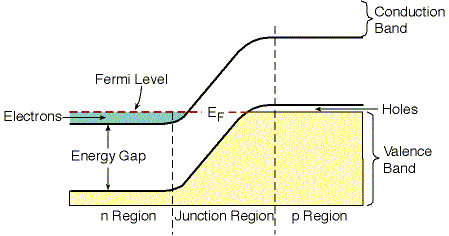
Figure 6.22 displays the energy bands of an ideal
p-n junction without any external voltage applied to it.
This arrangement of the energy bands in the junction is the basis for
the diode laser action.
The maximum energy level occupied by electrons is called Fermi
Level.
When the positive contact of the voltage is connected to the p side
of the p-n junction, and the negative voltage is connected to the n side,
current is flowing through the p-n junction. This connection is called
Forward Biased Voltage.
When the reverse polarity is connected, it is called Backward
Biased Voltage, and it cause an increase of the potential
barrier between the p side and the n side. Thus preventing the current
flow through the p-n junction.