Rami Arieli: "The
Laser Adventure" Chapter 6.3 Diode lasers Page 7.
Applying Voltage over p-n junction
When voltage is applied across
the p-n junction, the population of the energy bands changes.
Voltage can be applied to the junction in two possible configurations:
-
Forward Biased Voltage
- means that the negative pole of the voltage is connected to the "n"
side of the junction, and the positive side is connected to the "p"
type semiconductor, as shown in figure 6.23:
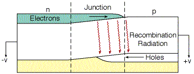 Figure 6.23: Energy band of a p-n junction which
is attached to a forward bias voltage.
Figure 6.23: Energy band of a p-n junction which
is attached to a forward bias voltage.
Forward biased voltage
creates extra charge carriers in the junction, lowers the potential barrier,
and causes injection of charge carriers,
through the junction, to the other side.
When an electron from the conduction band in the "n" side is
injected through the junction to an empty "hole" in the valence band on
the "p" side, a process of Recombination
of (electron + hole) takes place. As a result of this recombination process,
energy is released.
For diode lasers we are interested in the
specific cases when this energy is released in the form of laser
radiation. A sharp increase in conductivity occurs when the forward bias
voltage is approximately equal to the semiconductor energy gap.
-
Reverse (Backward) Voltage
- which causes an increase in the potential barrier of the junction, and
lowers the possibility for an electron to cross the junction to the other
side. Increasing the reversed bias voltage to high values (tens of volts),
can cause a voltage breakdown (Avalanche) of the junction.
If you want to play with an interactive simulation about the energy
level diagram of a Diode Laser, click here.
(VQM Simulation - Diode Laser)(Requires Shockwave)